Research
Engineering and probing nanoscale functionality in van der Waals quantum materials
Future quantum, photonic, optoelectronic, and sensing technologies require materials in which light, charge, excitations, and polarization can be controlled at the nanoscale. Van der Waals materials provide a versatile platform for this goal: they are atomically thin, stackable, twistable, strainable, and highly sensitive to edges, defects, vacancies, and local symmetry.
In these systems, functionality is often governed by atomic-scale structure. Small changes in stacking, strain, curvature, twist angle, edge geometry, or defect configuration can reshape excitons, plasmons, band gaps, polarization textures, and quantum-emitter behaviour. Our research combines materials design, electron nanoscopy, spectroscopy, and machine-learning-based analysis to quantify how nanoscale structure gives rise to optical, electronic, polar, and quantum functionality.
Materials platforms and nanoscale design
How can materials architecture be used to create new functionality?
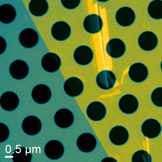
We design low-dimensional van der Waals systems by controlling stacking, twist, strain, curvature, edges, defects, and material combinations. These platforms — including heterostructures, nanotubes, nanoscrolls, patterned structures, and device architectures — allow us to study how nanoscale design shapes optical, electronic, polar, and quantum responses.
Electron nanoscopy and spectroscopy
How can we measure structure, fields, and excitations where functionality emerges?
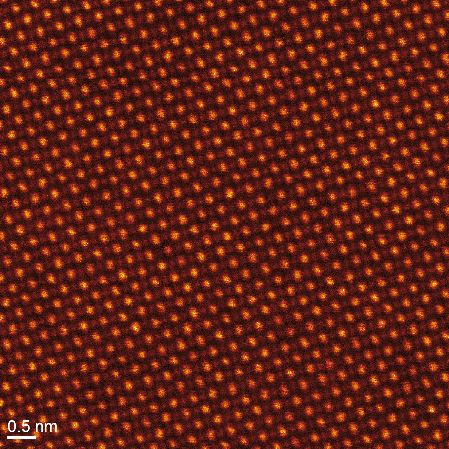
We use electron nanoscopy to probe van der Waals materials at atomic and nanoscale resolution. STEM, EELS, momentum-resolved EELS, and 4D-STEM allow us to connect local structure with strain, electric fields, polarization, excitations, band gaps, and plasmonic responses.

Machine learning for quantitative microscopy
How can complex microscopy data be converted into reliable physical quantities?
We develop machine-learning-based analysis methods to extract quantitative, interpretable, and reproducible information from EELS and 4D-STEM datasets. Our goal is to transform complex measurements into reliable maps of local material properties and structure–function relationships.

Translate
From vdW quantum materials to quantum technologies
How can engineered van der Waals materials be integrated into future nanophotonic and quantum devices?
We explore how low-dimensional van der Waals materials can be integrated with chip-compatible nanophotonic platforms. This direction connects materials design, electron microscopy, and spectroscopy with applications in single-photon emitters, nonlinear nanophotonics, and quantum communication.
A complete list of publications from our group can be found on the Publications page.