Electron Microscopy for 2D van der Waals Materials
The study of 2D van der Waals (vdW) materials demands highly specialized techniques to unravel their complex electronic and structural properties at the atomic scale. These materials exhibit fascinating phenomena due to their reduced dimensionality and unique interlayer interactions, making it essential to use advanced electron microscopy techniques. In our group, we focus on Electron Energy Loss Spectroscopy (EELS), Momentum-Resolved EELS, and 4D Scanning Transmission Electron Microscopy (4D-STEM) to explore these materials in depth.
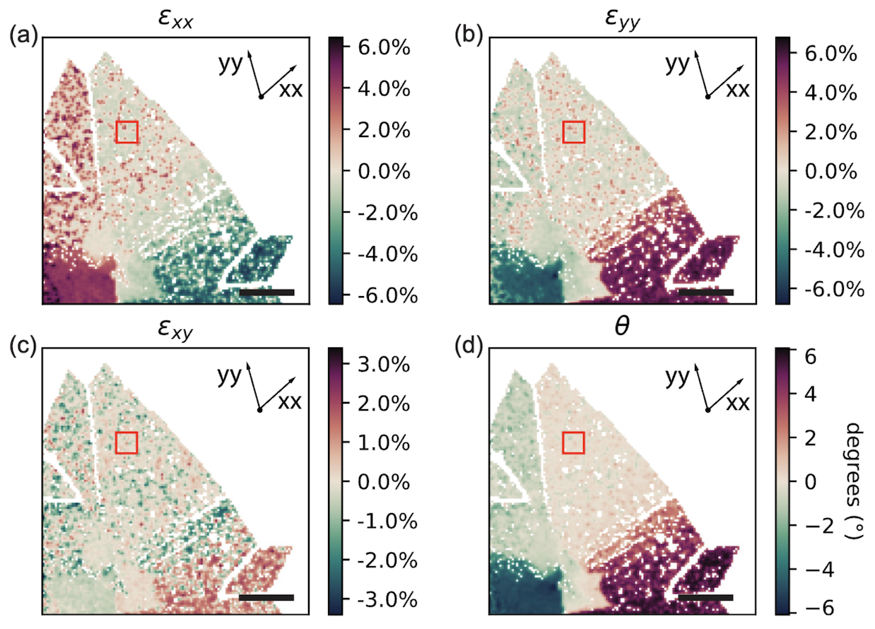
Strain and rotation maps of a MoS₂ thin film nanostructure. [M. Bolhuis et al., 2024]
EELS is used to probe the electronic structure of 2D vdW materials by measuring the energy loss of electrons. This provides essential data on bandgap modulation, dielectric properties, and electronic excitations. These insights are key to understanding the potential applications of vdW materials in areas such as optoelectronics and quantum technologies.
Momentum-resolved EELS adds another dimension to our analysis, allowing us to investigate the momentum transfer during electron interactions with the material. This technique provides detailed information on the dispersion relations and collective excitations like plasmons and excitons, helping us to understand how electronic states evolve with momentum, which is particularly important for 2D materials and their anisotropic behavior.
4D-STEM combines high-resolution imaging with diffraction data, allowing us to map strain, atomic displacements, and electric fields at the nanoscale. This method is invaluable for visualizing and quantifying the structural deformations and strain effects in 2D vdW heterostructures, which influence their overall electronic and mechanical properties.
Together, these techniques provide an unparalleled view into the underlying mechanisms that govern the behavior of 2D van der Waals materials, enabling us to design and optimize materials for future applications in quantum computing, sensing, nanophotonics, and energy-efficient devices.
To support the advanced analysis required for these electron microscopy techniques, our group has developed Python-based, open-source frameworks. Specifically, we have created EELSFitter for the precise analysis and interpretation of EELS, enabling automated extraction of key electronic properties and excitations. For 4D-STEM, we have developed StrainMApper, a powerful tool designed to accurately map strain and structural distortions at the nanoscale. These frameworks incorporate machine learning algorithms to enhance data processing and interpretation, and are freely available to the scientific community to promote collaboration and innovation in 2D vdW materials research.
Publications
For further reading on our work in Electron Microscopy for 2D vdW materials, please refer to the following selected publications:
- Nanoscale Strain Mapping in van der Waals Materials from 4D-STEM: Beyond the Planar Configuration. M. Bolhuis, S. E. van Heijst, J. J. M. Sangers, S. Conesa-Boj [Small Science 4, 2300249 (2024)]
- Heterostrain-Driven Bandgap Increase in Twisted WS2: A Nanoscale Study. S. E. van Heijst, M. Bolhuis, A. Brokkelkamp, J. J. M. Sangers, S. Conesa-Boj [Advanced Functional Materials 34, 2307893 (2024)]
- Localized Exciton Anatomy and Band Gap Energy Modulation in One-Dimensional MoS2 Nanostructures. S. van der Lippe, A. Brokkelkamp, J. Rojo, S. Conesa-Boj [Advanced Functional Materials 33, 2307610 (2023)]
- Edge-Induced Excitations in Bi2Te3 from Spatially-Resolved Electron Energy-Gain Spectroscopy. H. La, A. Brokkelkamp, S. van der Lippe, J. ter Hoeve, J. Rojo, S. Conesa-Boj [Ultramicroscopy 254, 113841 (2023)]
- Spatially Resolved Band Gap and Dielectric Function in Two-Dimensional Materials from Electron Energy Loss Spectroscopy. A. Brokkelkamp, J. ter Hoeve, I. Postmes, S. E. van Heijst, L. Maduro, A. V. Davydov, S. Krylyuk, J. Rojo, and S. Conesa-Boj [J. Phys. Chem. A 126, 1255 (2022)]
Team Members
Abel Brokkelkamp, Kavli Institiute of Nanoscience, Delft University of Technology
Jeroen Sangers, Kavli Institiute of Nanoscience, Delft University of Technology
Sonia Conesa Boj, Kavli Institiute of Nanoscience, Delft University of Technology